Introduction to the Microbug
This lab will be a bit longer compared to the previous two, and a big step up in terms of complexity.
You will be making the schematic and layout of a small programmable robot. Below is a video of a robot very similar to the one we want to make:
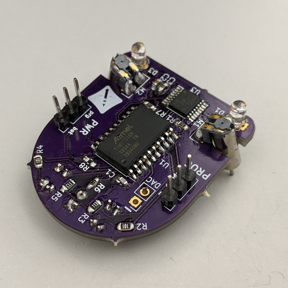
The microbug is a small, simple robot with reflectance sensors and high-speed motors. It's got an ATTiny microcontroller for brains, an LED caster, additional LEDs for the bug-eye look, and multiple power options. Originally meant to be a replacement to the USB Charger lab, the idea for the microbug came from the desire for a PCB that would fun to keep around and show off.
There are quite a few things that are new with this project:
- Using a microcontroller
- Importing a board shape from mechanical CAD
- Very limited board size - using both sides of the board
- Using non-standard parts on a PCB (motors)
- Importing graphics
- Preparing for expandability
Parts and Schematic
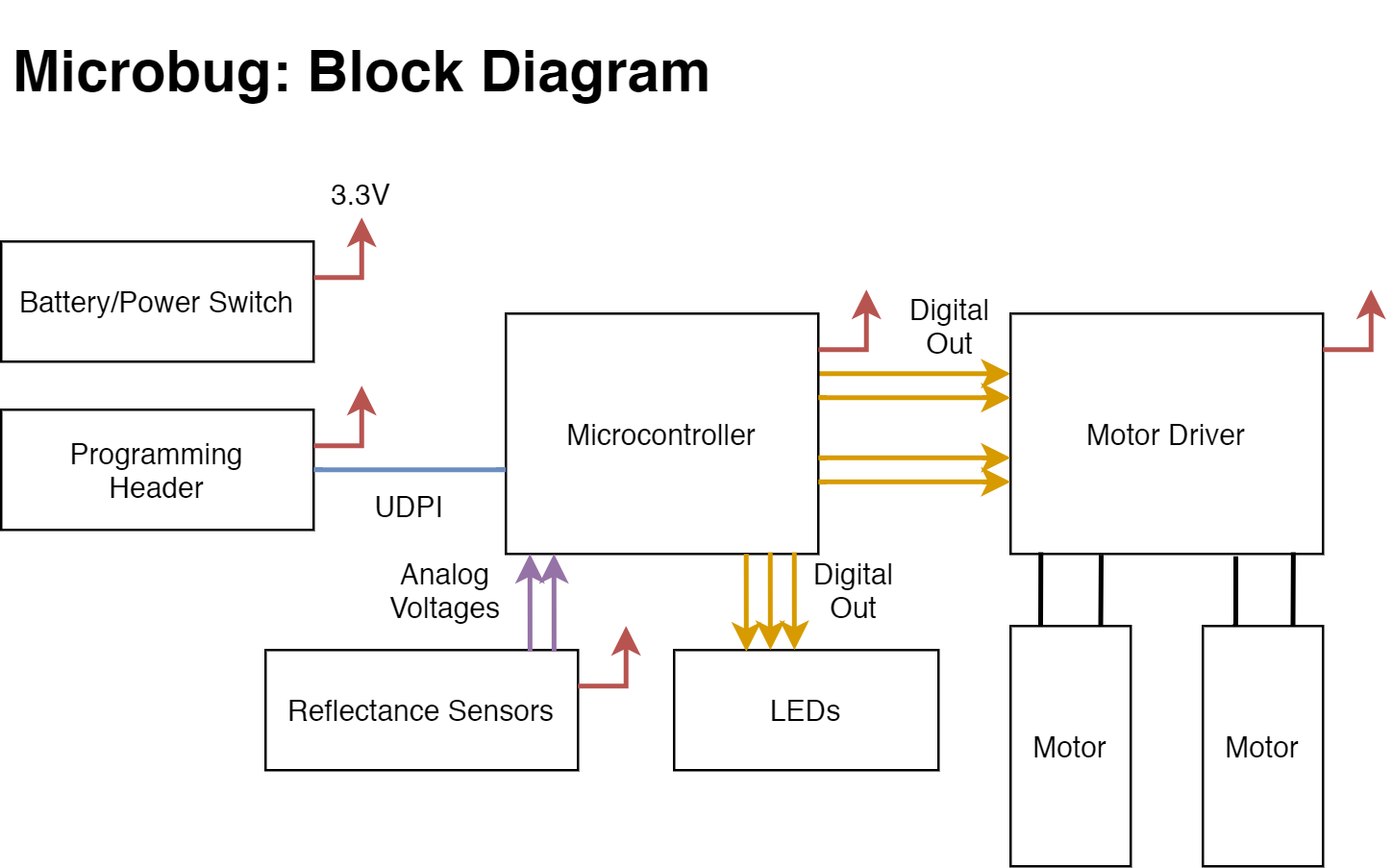
Below is a basic block diagram of the robot; we expect your schematic to somewhat resemble this (but you don't need to draw wires between the blocks if using labels is neater). Integrating the input pins (programming, power) together is fine, as is reorganizing the diagram, as long as it makes sense and represents the same overall purpose in the end.
These are an example of the main “blocks” in your schematics:
- A microcontroller block (micro and power filter passives).
- A motors and motor controller block (and power filtering passives).
- A sensing block (the reflectance sensors and its passives)
- An LED block (LEDs and their passives)
- A programming header block
- A power block
For the basic parts we’ll be using these:
| Part | Detail |
|---|---|
| Microcontroller | ATtiny1616, the brains that will actually control the motors and read the sensors and make decisions |
| Reflectance Sensors | QRE1113GR, for seeing changes in brightness underneath it, like for following a line |
| 3x LEDs | as indicators/blinky lights back to the user |
| Battery | The main power option will be a CR2032 coin cell battery, you’ll need to find a battery holder for a CR2032 cell and possibly need to make a custom footprint for it. You should also include a 2-pin header for alternative power. |
| Motor Driver | TC78H651AFNG (or TC78H660FNG, if you want a bit more of a challenge), to be able to supply high currents to the motors |
| Motors | To move around; just use a generic motor symbol for now in schematics, for layout you’ll need to later make a footprint that we will give dimensions for. |
Supporting passives and other connectors will be up to you to find. If you aren't sure what some passives values might need to be, or what sizes seem reasonable, check their datasheets closely, and look for existing product implementations online that use that part.
When you are finding and compiling your list of parts, don't forget to record them in a BOM. You may find that some parts do not have a symbol from the built-in symbol libraries. Follow the datasheet and make your own / import from online in a new project symbol library.
Note: we know that the first listed motor driver above is out of stock everywhere. For the purposes of this assignment, don't worry about it.
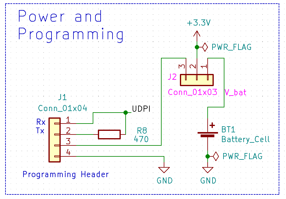
Programming and Power Control Header
We use an unorthodox way of programming the microcontroller and switching power. The J2 connector acts as a psuedo Single Pole Double Throw switch, which we implement with a pinheader jumper to swap where the 3.3V comes from. J1 is the programming header. To keep things simple, we provided the schematic these two connectors below:
Layout
Motor Footprint
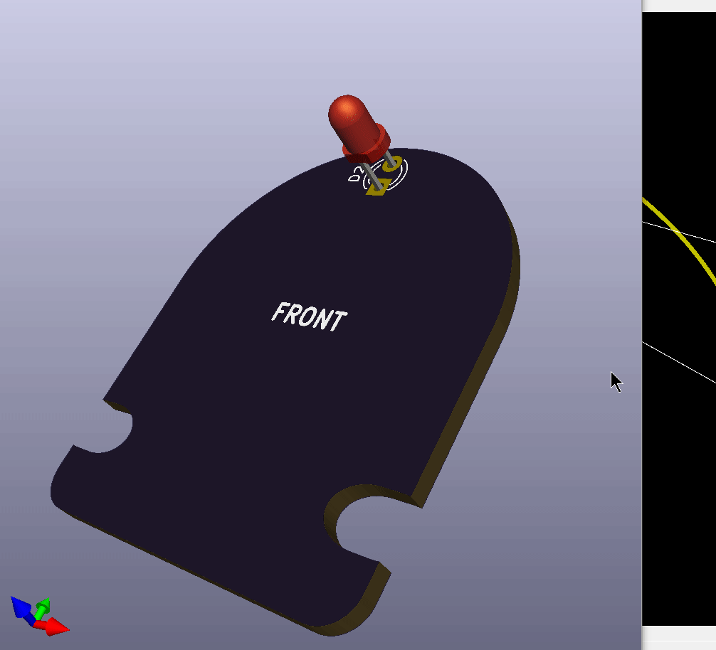
The motors are these tiny DC motors that Jeffrey found from some seller on ebay, and we thought they would be perfect for a little skittery robot. Note that we remove the square shell in assembly, hence the circular cutouts in the board.
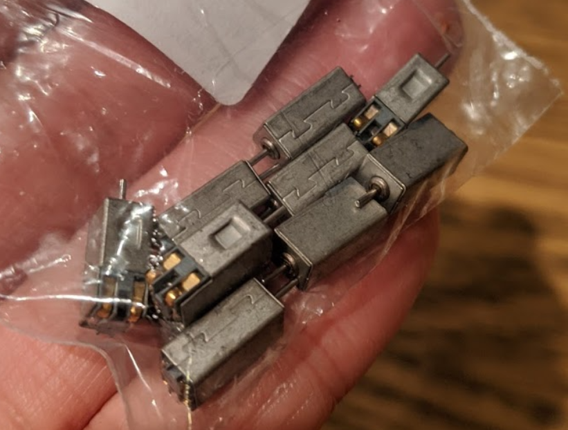
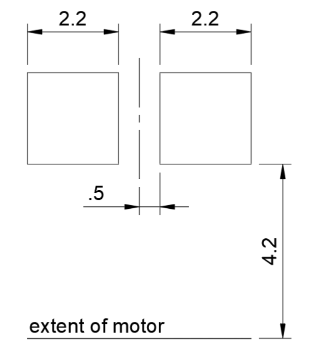
To connect the motors to the boards, they fit in the round cutouts on both sides of the board, with the side of the motor with the exposed contacts facing the board surface. Thus, the required footprint for the motors is simple: just two large pads for the motor contacts. The pads are the squares, and dimensions are in mm in the drawing below. You should additional appropriate footprint layers.
Complete the layout
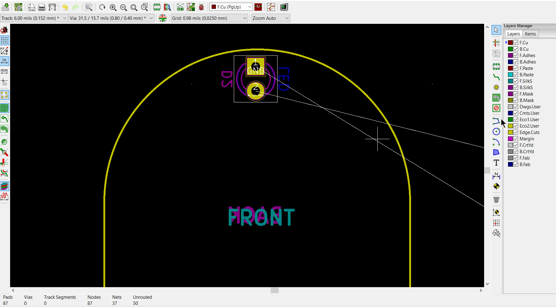
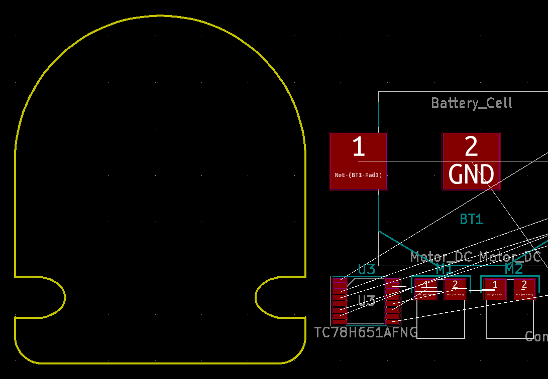
You are provided with the board outline, which comes as a .dxf file. IMPORT THE BOARD OUTLINE BEFORE PLACEMENT OR ROUTING.
We highly, highly suggest searching up the datasheets for the parts we choose to understand what they are supposed to do, and faciliate part placement and orientation in relation to the board outline. Not all part placement rules are specificed below. Understanding how things should be oriented is part of the lab. For example, take a look at the battery cell holder on Digikey.
- Make sure it falls under BAC's standard capabilities just like in your last design (USB Charger lab).
- You are allowed and encouraged to use both sides of the board.
- Standard 2 layer board. You are not allowed to design with more than 2 layers.
- You MUST use the provided board outline and component footprints.
- Exception: you are allowed to change the footprints for the 2 LEDs not being used as the rear caster.
- Try to minimize the number of vias used. A suggested maximum is 20.
- One of the LEDs must go on in center of the back of the board, facing downwards. It acts as the caster for the robot.
- All pin headers should be facing up.
- The other two LEDs should be visible from the top of the PCB.
- The two light sensors must be facing downwards on the left and right sides of the caster LED in the back. They are meant to be used as sensors for line following.
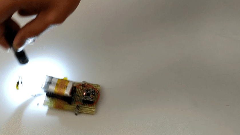
- Motors must be mounted at the two cutouts at the flat "head" end of the board. You should try to align the center of the pads as nicely as you can with the rounded cutouts. Take a look at the gif to get a general idea of how the motors are expected to be mounted. Note that the motors the board outline was made for are round.
- Add the IEEE logo (provided as an image) somewhere on the board with a reasonable size. Instructions below for how to create footprint from bitmap. As with all silkscreen elements, do not have it overlap pads, board edges, or other silkscreen.
- We also highly suggest adding additional silkscreen to label important connections). One connector is meant to be used with a jumper, can you figure out which one it is?
Checkoff: We're going to be checking for all of the above, in addition to a completed layout with no DRC errors, and BAC InstantDFM report.
Important (and late) note: There is one unconnected error that we expect to be in your completed board layout. Hint: look at the datasheet for the battery holder.
How to Import the Board Outline
Download the board outline from here. If you cleverly set your grid size you can get things to line up nicely using the properties panel.
- In the Pcbnew layout editor:
File -> Import -> Import Graphics. Then select themicrobug_body.dxf. - Under 'DXF parameters' make sure that default units are set to 'mm' Note: This is not the same as changing the units of the pcb editor itself! (This step is needed because the .dxf file was exported in mm units)
- Change the graphic layer to "Edge.Cuts" then click OK.
- Click to set down the imported board outline. It should look like so: (placement arbitary, only to show proper imported size)
How to flip parts to the other side of the board
The rear caster LED is required to be facing downwards along with the two light sensors, and we suggest having the battery holder on the bottom as well.
Note: Text SHOULD BE mirrored when on the back.
- Hover over the part you want to flip to the other side of the board, then press
F(orRight-Click -> Flip). - That's it. Notice how the colors of the footprint silkscreen changes from the color for the top to the color for the bottom.
How to insert images
Silkscreen art? Copper art? Just, boring logos?
- In the main KiCad project window, find the Bitmap to Component Converter (looks like a lowercase 'a' being measured).
- Click "Load Bitmap" and select the desired
bitmap. For this lab, the "ieee-logo.bmp"image. For this lab, the "ieee-logo.png" should be in folder named "logos" from the same Drive folder linked above for the board outline. For some reason, the Bitmap to Component Converter has broken importing actual bitmap images, but other file types such as .png seem to work fine...
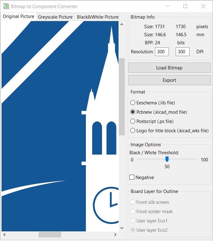
- Note that the imported image is huge (146.6mm by 146.5mm). You can resize by:
- Making the image smaller externally, like in Photoshop or something.
- Change the Resolution (in Bitmap info, right above the "Load Bitmap" button). Increase the values to have the resulting footprint appear smaller, and reduce to make it bigger. DPI stands for "dots per inch".
- Keep format in Pcbnew (you're going to make a footprint object essentially), and select "Front silk screen" in the "Board Layer for Outline" section.
- If want to do exposed copper art, you should use the "Front solder mask" option. Don't do this for this lab.
- Click the "Export" button and save the footprint (.kicad_mod) file into the "microbug-fplib.pretty" folder in the project directory.
- Import the footprint directly in Pcbnew, or add a placeholder, no-pin symbol in the schematic and assign as footprint.