In this KiCad activity, we will design a printed circuit board (PCB) for an LED light sensor.
This lab is meant to be a guided, rapid intro walkthrough of the minimum processes needed to make a complete PCB in KiCad. If you don't understand every step here, don't worry! Future content will cover each step more in depth.
Getting Started
-
Launch KiCad. You should be greated with the main project manager window.
-
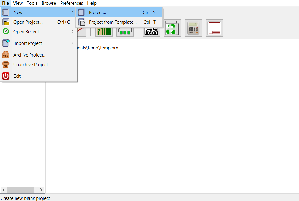
Make a new project by
File -> New -> Projector by using the keyboard shortcutCtrl-N. Pick reasonable project name (i.e. light sensor) and a safe place to save your project directory (a folder will be created to house all your KiCad project files)You won't be able use KiCad as a comprehesive PCB ECAD unless you're working under the context of a project, so make sure to do this step!
Schematic Capture
- Open the 'Schematic layout editor' aka the 'Eeschema' app (1st from the left).

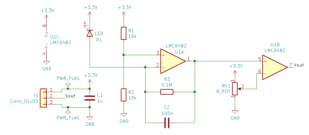
- All you have to do is simply replicate the KiCad schematic below:

Parts and Wiring
-
The first thing we want to do is add the components: resistors, op-amps, etc.
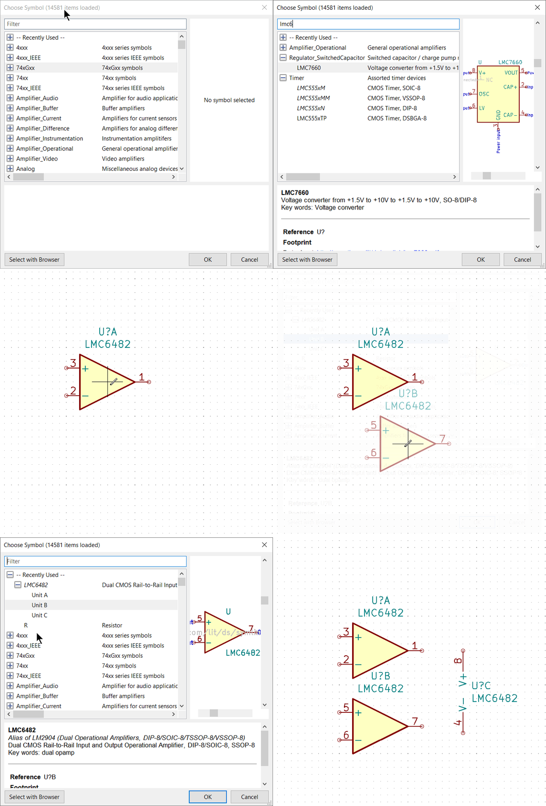
- Press 'a' to bring up the parts Symbol library (or click the little op-amp in your right side-bar, then click anywhere in the schematic).
- In the filter bar, type 'LMC6482' to find the component. Open the drop-down and select 'Unit A'.
- Place the unit on the schematic. Repeat with 'Unit B' and 'Unit C'. Place 'Unit C' only once. Press 'ESC' to exit insert mode.
Interested in why the op-amps come as these separate units of one part? Take a look at page 18 of the LMC6482's datasheet to get some idea of why the component would be set up this way.
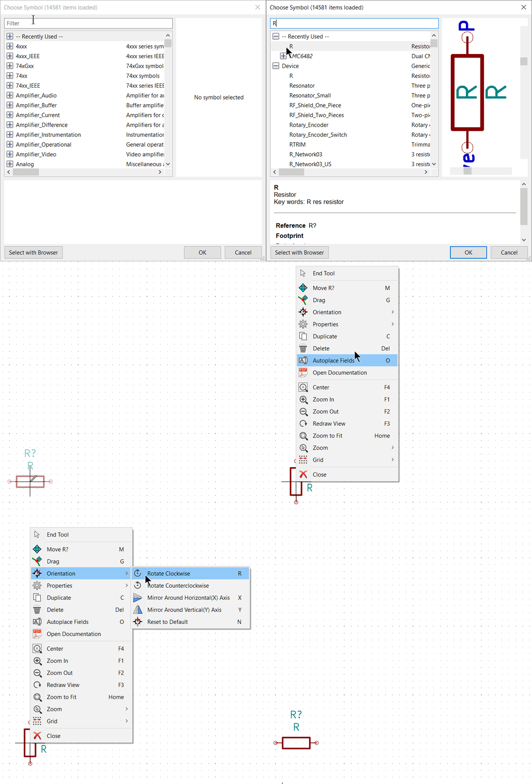
- Open the part symbol browser (remember you can access this by clicking 'a') and search for 'R'. Find the generic resistor part symbol.
- Place 3 resistors as shown in the schematic.
- To rotate before placing, press 'r' before placing the component. Hovering over a placed component and using 'r' will also rotate it. You can move components around by using 'g'.
-
Right click on any component to look at the other editing options available.
Go to
Help -> List Hotkeys... or press Ctrl+F1 (Win) to open up KiCad's built-in keyboard shortcuts cheat sheet! Note that the middle mouse can be used to drag your view in both the schematic and layout editor. This will help alleviate the headache of trying to scroll around both.
-
Continue by placing the following parts to match the completed reference schematic:
-
two capacitors ('C')
-
a LED part symbol ('LED')
-
a potentiometer part symbol ('R_POT')
-
a 1×3 connector part symbol ('CONN_01x03') - should be listed as generic
-
At this point, you can either continue to step 4, which involves wiring, or you can stop and organize your schematic. You can place the components listed above, as well as those from previous sections to match the schematic below.
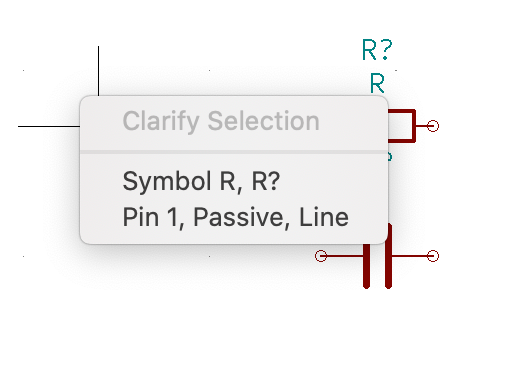
You might see something like this while placing components on your schematic. This happens when you click a component that either might be stacked too closely with another component or you click a specific pin instead of the entire component. Select the item you would like to edit from the dropdown and continue!
The following instruction is for wiring. Feel free to do step 7 first
to get all pin-symbols on the schematic before starting to draw wires. If you are unsure, continue with this step.
-
To connect components: move your mouse to where you
want to start a wire, press 'w', click around to snap wire, and click on
a pin to end the wire. You might see the dropdown mentioned above when selecting a pin on a component. In this case, make sure to select the option with the pin and not the entire component itself.Repeat until the schematic is fully captured.
-
Drag placed wires by hovering over them and pressing 'g'. Delete segments
by pressing 'Backspace' or 'Del', or right click the wire for more options. -
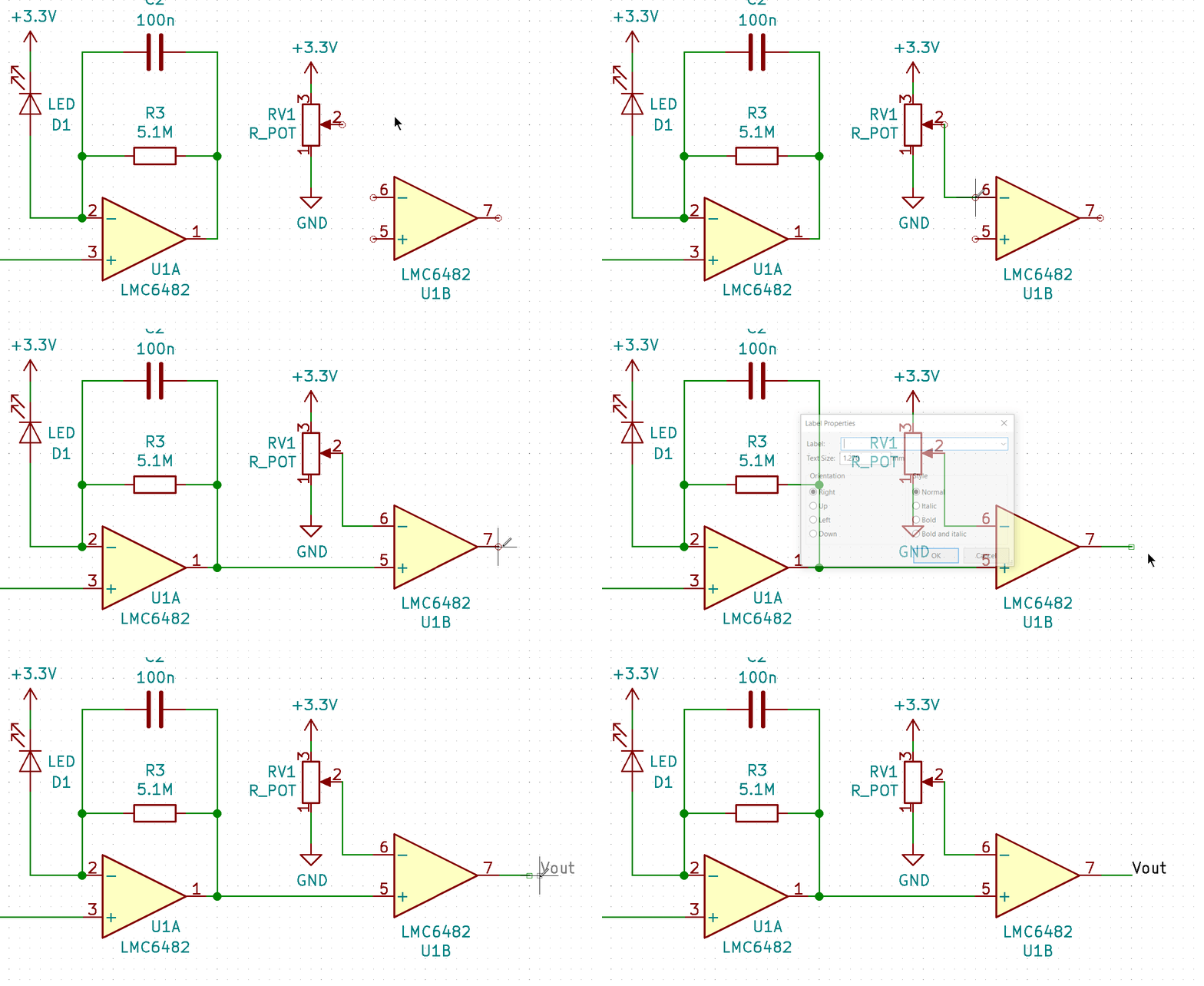
To create a wire that does not connect to a component on one end
(floating wire), double click where you want the wire to end. Floating wires will be useful for components that will need power or ground labels later. -
To add labels (the 'Vout' label shown above), press 'l' and type in the
name of your label. Labels connect two or more nodes together without
actually drawing the wire on screen. They are basically magic wire tunnels
linked by name. -
Note that these wires do not snap to component pins. If you move or
rotate a component, its seemingly connected wires will not follow.
-
-
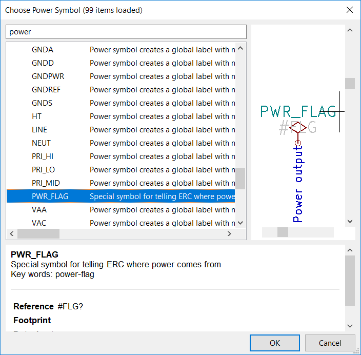
Now add power symbols to your schematic. Get these from the power symbol
window by pressing 'p' or finding its icon (a GND symbol) in the right toolbar.-
5 voltage sources labels ('+3.3V')
-
4 ground power labels ('GND')
-
Power flags ('PWR_FLAG')
-
For this step, it may be easier to duplicate a component instead of adding multiple of the same component. To do this, hover your cursor over the component you want copied and press 'c'.
-
Assign component values to components. For each resistor and capacitor, mouse over and press 'v'. The easiest way to find this menu is to double-click the component. You can also find it in the 'Properties' section of the right-click menu. In the 'Text' field, type the appropriate value. Omit units (F for farads, H for Henries, etc.).
-
Assign unique numbers to each component. You can do this in the same menu as above, or automatically by using
Tools → Annotate Schematic → Annotate.Feel free to use these interface menus to learn more about KiCAD's functions, or even for this entire first lab. However, we do recommend learning how to use the keyboard shortcuts, as doing so will speed up your work in future projects considerably. Also, you'll look much cooler.
Footprint Assignment
What should have been completed so far is the circuit schematic. That is, we have transcribed our circuit's components and their connections into a format that KiCad, and hopefully others, can understand. Now, we need to tell KiCad what each of our parts look like physically on the board. First, we need to assign what each component actually looks like in the real world. Or at least, how they will look on our PCB. These representations are called footprints.
If you'd like to see a quick tutorial and walkthrough of how to assign footprints, check out the video below. If not, continue forward with the steps.
- Go to
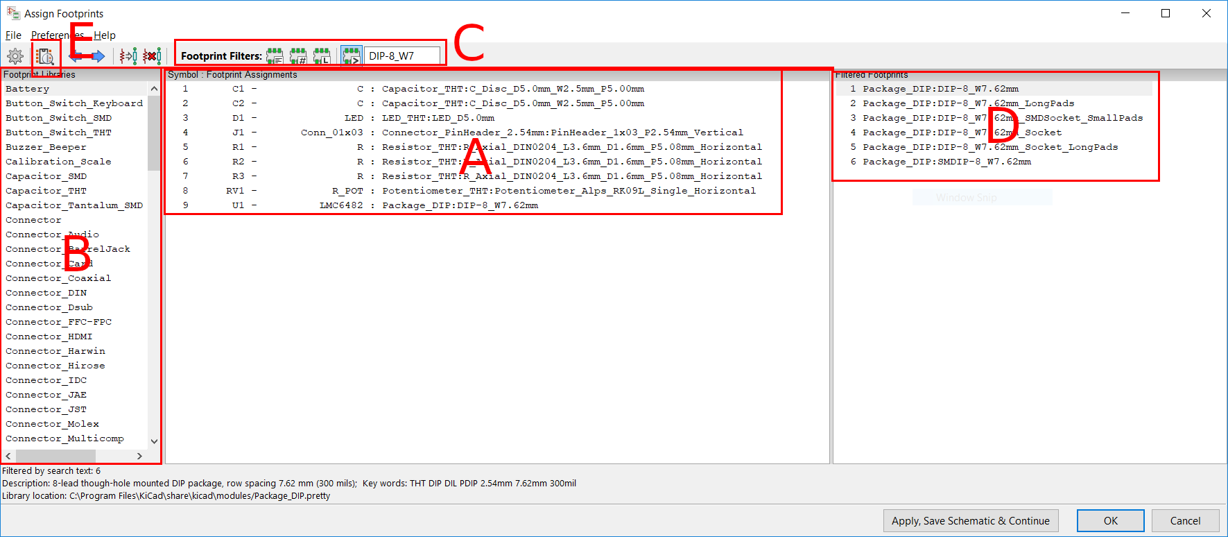
Tools → Assign Footprints. Note that it may take a while to open as KiCad loads in all the footprint libraries. We have labeled the different sections of the window from A - E for your ease in following our instructions.
-
Pick the first unassigned footprint from A. If you want to assign multiple components with the same footprint, select multiple components using SHIFT-select.
-
In B, select the component library from which you want to select your footprint. For example, for components C1 and C2, you would probably choose either libraries "Capacitor_SMD" (surface-mount capacitors) or "Capacitor_THT" (through-hole capacitors).
-
Activate the footprint filters in C. Filter by the library "L" and the number of pins "#". You can further narrow down your search by adding keywords in the text box to the right.
-
Select the appropriate footprint in D. Press E to preview selected footprints. Make sure to double-click the footprint in the right panel to assign it. If you accidentally assign the wrong footprint, select the assignment in A again, and reselect in D.
-
Repeat these steps until all footprints are assigned.
-
Press "OK" to save and dismiss the window. Do not click "Apply, Save Schematic & Continue"
We recommend using the following footprints:

PCB Layout
PCB Layout Setup
If you'd like to see a walkthrough of how to layout your PCB, check out the video below. It goes through the entire process of PCB layout. If not, continue forward with the steps.
- Inside the schematic layout editor, go to
Tools → Update PCB From Schematic. This should open up the Pcbnew window and a popup window. Click 'Update PCB'
If you get the warning: "Cannot update the PCB, because the Schematic Editor is opened in stand-alone mode. In order to create/update PCBs from schematics, you need to launch Kicad shell and create a PCB project.", just open the application Pcbnew in a new window and continue.
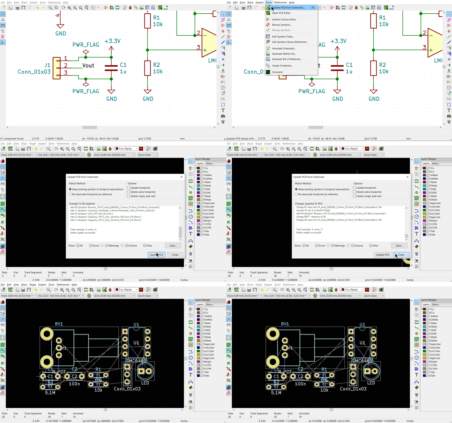
If you've done everything correctly so far, there should be no errors in the
"Update PCB from schematic" window, as shown above. Your PCB layout window
should have opened up and should look like this:
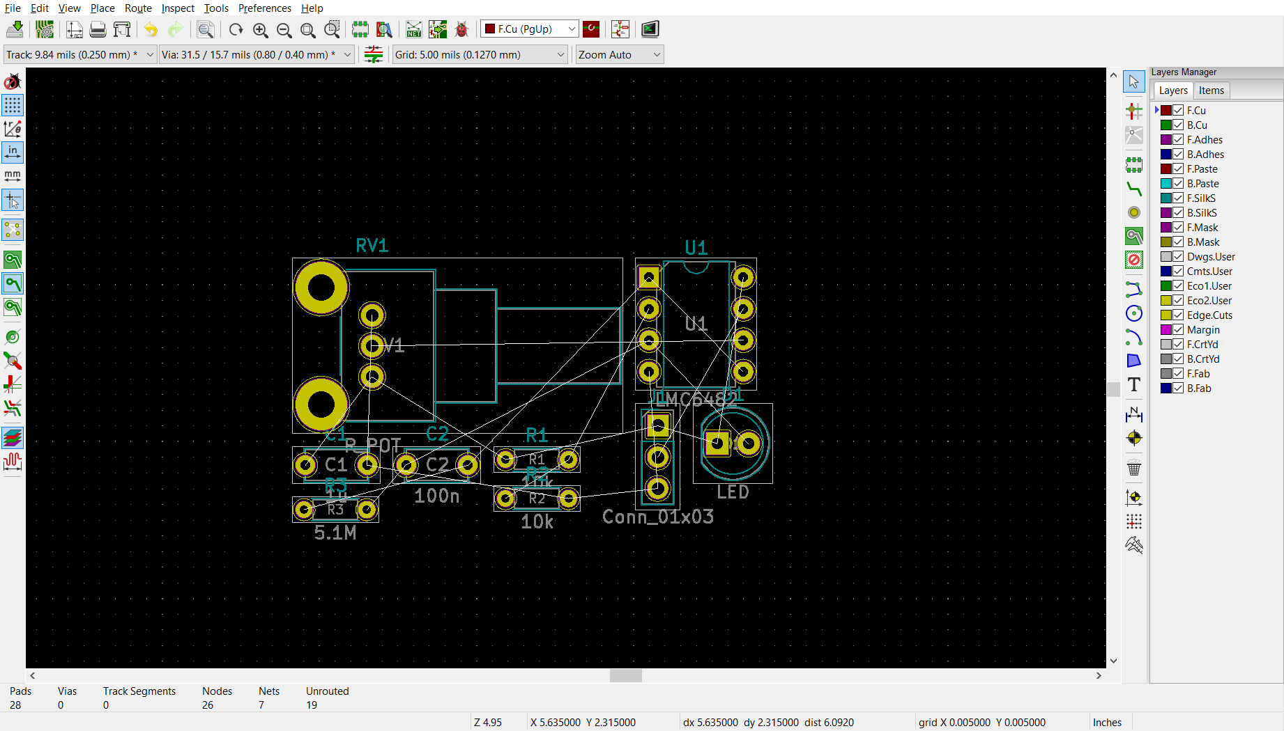
Click somewhere in the PCB layout editor window to place all the
imported footprints.
Now, let's do some basic environment setup before we actually getting started.
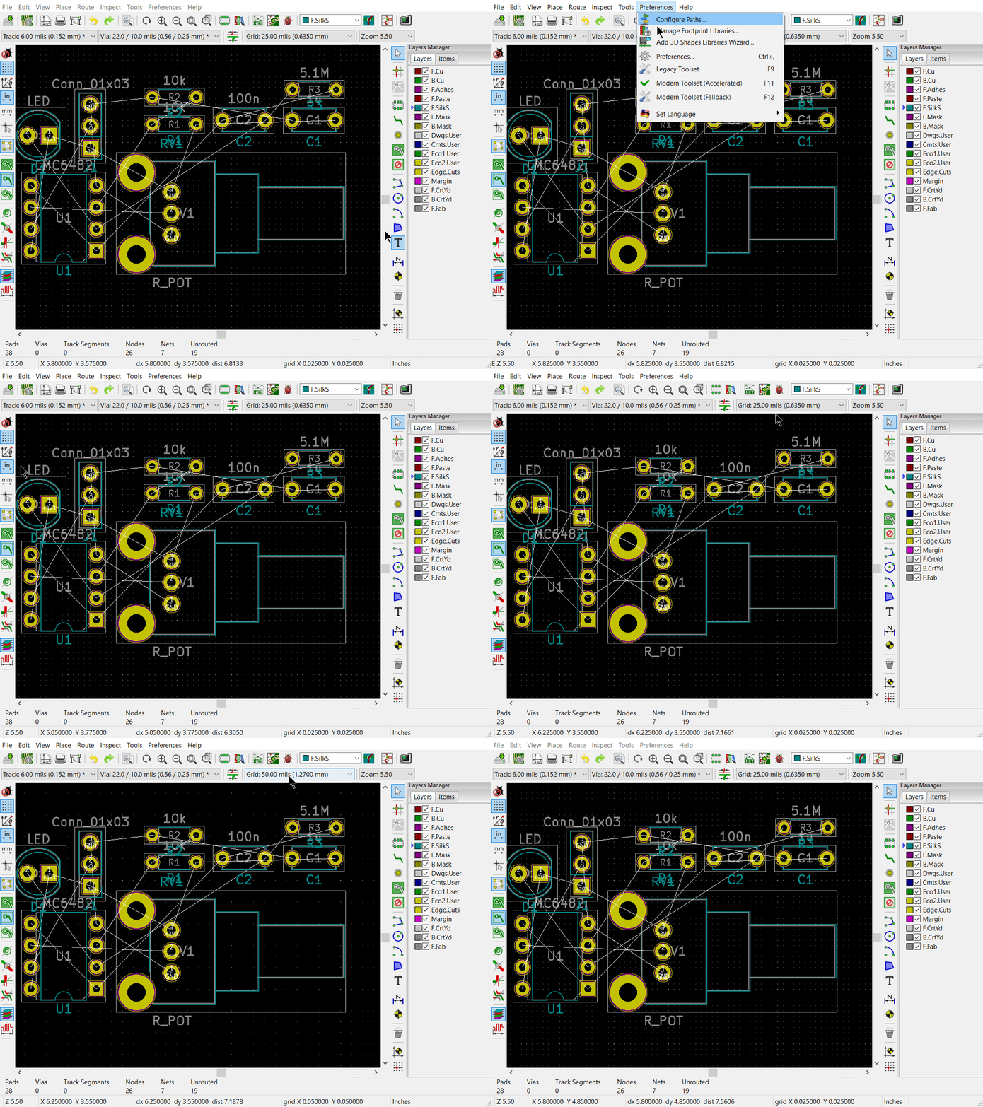
- Make sure that you are using the Modern Toolset. Preferences → Modern Toolset (Accelerated).
- Also make sure that you are set up to use inches. Press the "in" button in the left sidebar. (Why the inferior imperial measurement system? Try searching around online if you're interested)
- Set your grid size (try a 50 or 25 mil grid). When working with others' designs, using a common grid unit size will help make sure your components and tracks line up with theirs.
-
Get to the board setup window by
File → Board Setup. Set Preset Layer Groupings to "Two layers, parts on front" in the 'Layers' page (default screen that the Board Setup should open with).For those with some PCB design experience, feel free to set your design rules such that your board will fall under Bay Area Circuit's Standard Capabilities
Placement and Routing
In the end, we want something that looks like this:
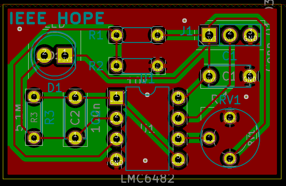
The red lines in the layout are called tracks or traces. They represent the physical connections defined by the connections made in the schematic doc.
Similarly, the red polygonal shapes are called fills, and represent large spans of copper that are also a way to represent wires in the schematic (usually power related wires).
The turquoise lines denote the silkscreen, which will be talked about later.
The gray boundaries denote component courtyards (F/B.CrtYd), or boundaries. Overlapping component courtyards will trigger a DRC error (if the rule is enabled) since two components are trying to occupy the same place.
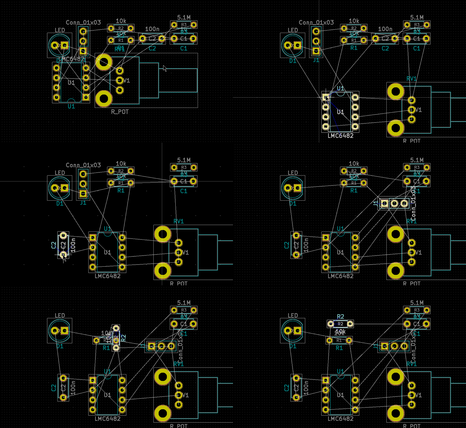
- First step is to move and orient components as you would like them to be on the board. It is recommended to position the op-amp IC first, and to keep the inputs/outputs accessible at board edges. Move components by mousing over them and pressing 'm'. To rotate, type 'r'. Click to place back down.
-
Finish placing the components on the board. Feel free to place them however you wish, but try to minimize the number of crossing white wires. These wires (called the "ratsnest") indicate intended connections as defined in the schematic.
Try disabling the view of the 'F.Fab' layer by unchecking its checkbox in the 'Layer Manager' window on the right. It will help make things look neater.
-
Swapping footprints: Let's say you're told that particular potentiometer won't work with the project, and you're told to swap it out with another, differently oriented potentiometer.
-
Go back to the schematic editor and reopen the 'Assign footprints' window.
-
Click on the potentiometer part in the footprint assignments, as reassign its footprint to be: "Potentiometer_Vishay_T7-YA_Single_Vertical"
-
Save, then re-update the PCB from the schematic. In the 'Update' window make 'Update footprints' checkbox is marked. You should see that the long potentiometer has changed to one that looks considerably different after the update.
-
-
Routing: drawing out the physical connections between the components. First, change your grid size to something smaller, such as 10 mil. Switch to the track tool via the button in the right toolbar or by using the keyboard shortcut 'x'. You need to route a physical track for each white line you see connecting different pins. Use the 'Highlight Net' tool to easily visualize to-be-made and made connections.
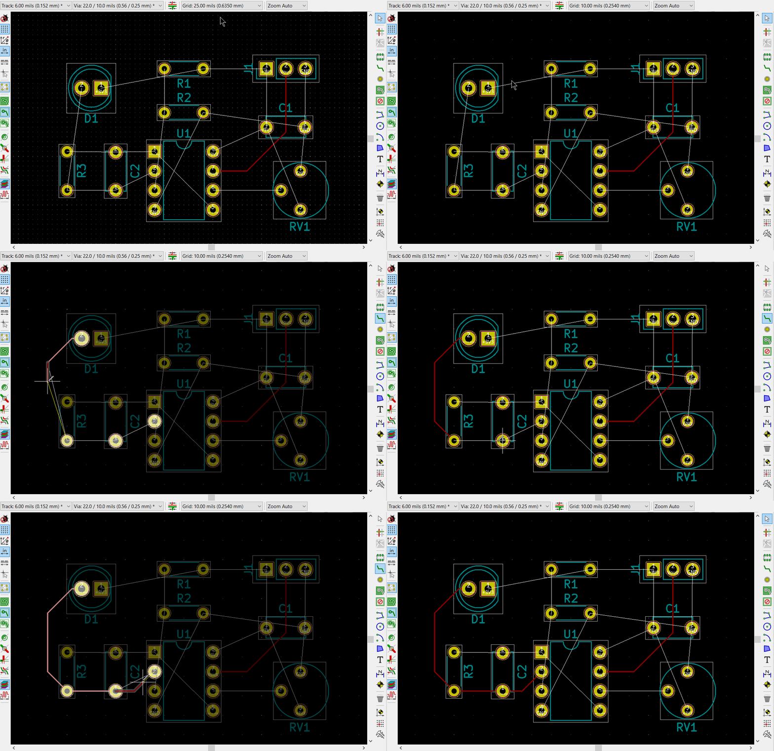
Don't worry too much about GND connections in your routing, and do the other connections first. Take a peek at the next step about ground planes to understand why!
-
Delete segments by pressing 'Backspace', or use 'Del' to delete the full track, or right click for more options.
-
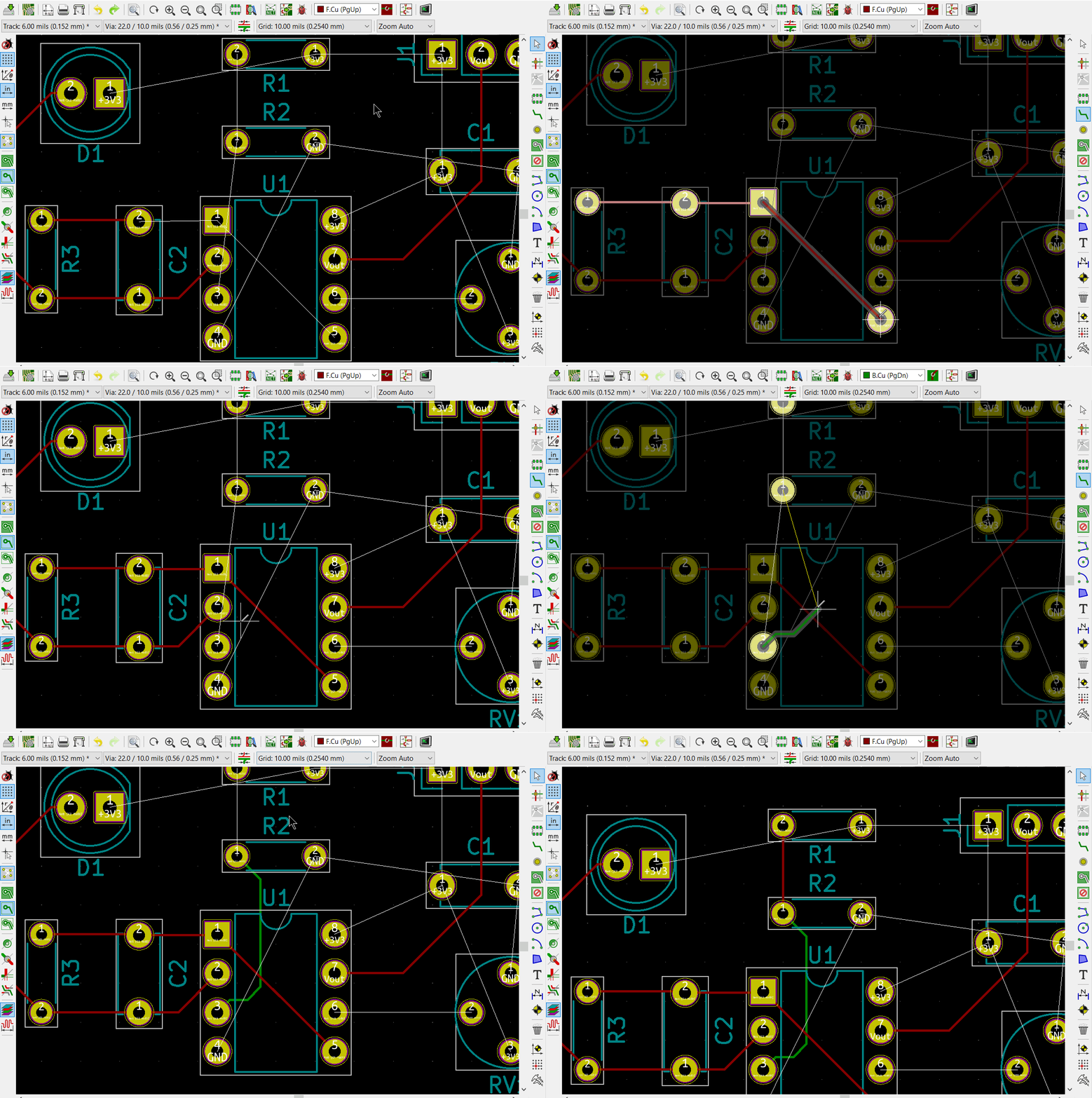
You may realize that one layer might not be enough to ensure no overlaps. Use func. key 'Page Down' to switch to the bottom layer. 'Page Up' will return you to the top layer. You can use VIAs (Vertical Interconnect Access), an electrical connection between multiple physical layers in a circuit board to connect traces on different layers. Note that because all the chosen component footprints are through-hole, that is, connected to the board via via like holes, independent vias are (ideally) unnecessary!
Vias are an available by: Pressing 'v' while in trace routing mode (i.e. you're in the middle of routing a trace and want to jump to the other layer) or using the 'add via' button in the right tool panel.
-
If you find it hard to draw out traces for all the connections, feel free to move and reorient the components themselves (or change them out completely, if you feel this is necessary). PCB design is an iterative process! Don't feel down if you have to restart completely. Routing PCBs is a very difficult problem after all (any kind of routing is in fact, a very hard CS problem). With practice, you will be able to arrive at more optimized layouts faster, and this course will go over some general practices and essential tips when approaching PCB layout.
Feel free to do whichever you want first: ground plane or edge cuts (board outline). Edge cut instructions can be found right after the ground plane instructions.
-
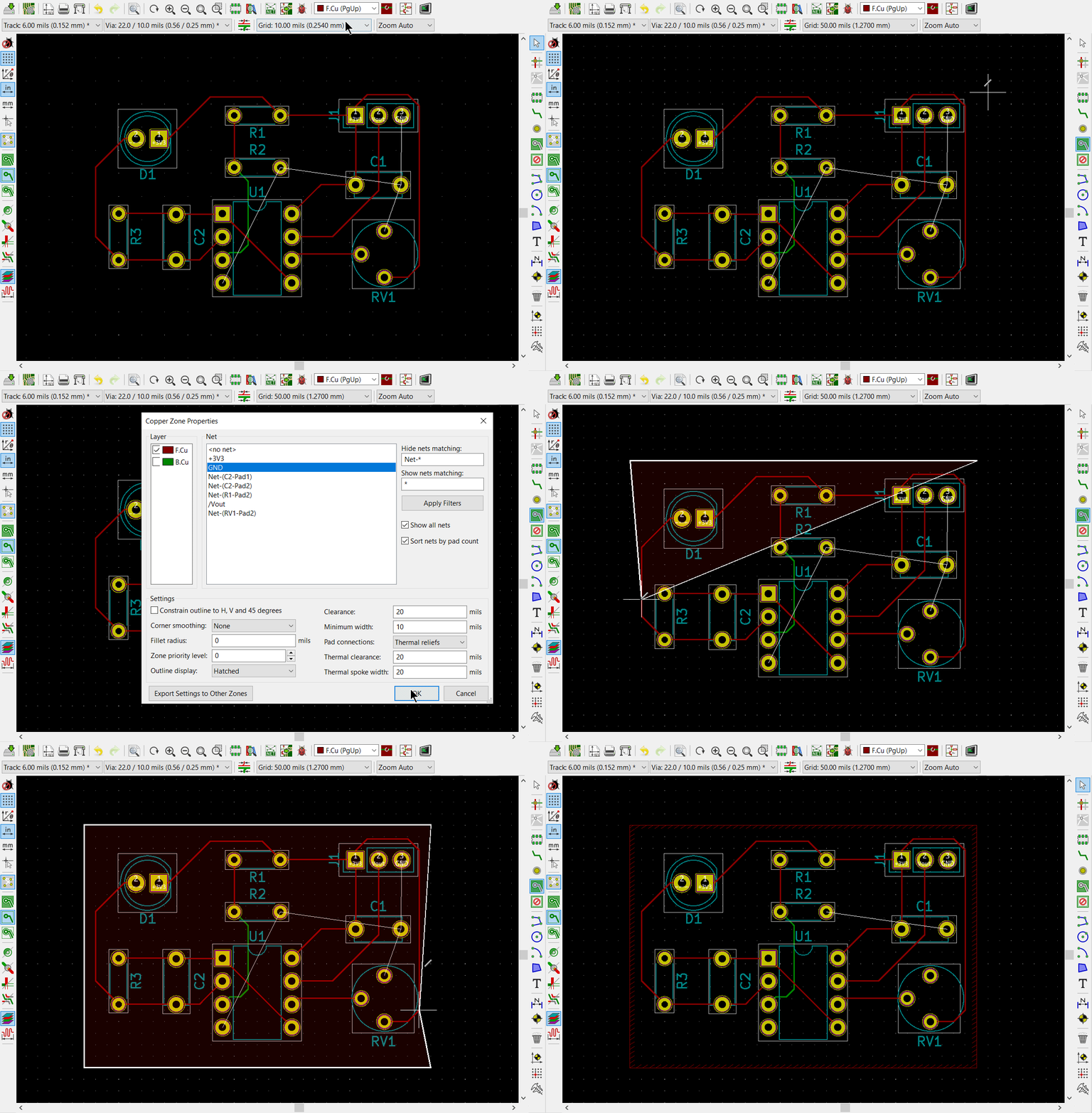
It is time to add a ground plane/ground pour to this board on both the top and bottom layers. A ground plane is a fill of copper dedicated entirely to the GND net. It is generally a good idea because it makes routing easier and reduces ground noise. To do this:
-
Set your grid size to something large, 50 mil+. This will make forming a neat pour polygon easier.
-
Click the 'Add filled zones' icon on the right-hand side toolbar then click on the screen where you want the first corner of your ground plane to be. A settings window should pop up. Select 'F.Cu'/'B.Cu' for Layer and 'GND' for Net. Don't worry about the other settings for now.
-
Draw the ground plane polygon. Make sure it encompasses all the parts and traces, make extend beyond your edgecuts, if you did them first. It does not hurt at all to go big, the edge cuts will "trim" it neatly for us.
-
Finish drawing the ground plane by clicking the other four corners of the polygon. Double click on the last corner to close the polygon.
-
-
Repeat the above steps again to make a second ground plane for the other
copper layer ('F.Cu' or 'B.Cu' that you have not yet done). -
If you update any other part of your board (add new traces, move a component,
etc.), press 'b' to re-fill all filled zones. If you find the filled zones
visually impairing, you can unfill with 'ctrl+b' or change how they are viewed.
Fill visibility buttons exist on the left toolbar, try to find them! -
Add edge cuts for the board. These are the physical boundaries of your board.
Select the 'Edge.Cuts' layer and, using the trace tool, draw a rectangle
that contains all the footprints and traces on your board. If you already did all
the ground planes, make sure that your edge cuts stay within the ground
polygons. You may choose to draw rounded corners, too, or other fancy shapes
for the board outline if you would prefer to.
-
Make sure that at least one of the ground planes (should be the one on the bottom layer) is not cut up too much by signal traces. Use vias to connect the top ground plane to the bottom. A good amount would be 1 via per ground island (if completely isolated planes of copper exist on the top layer).
-
You're almost done! Add to the board silkscreen (the identification layer). This is the (usually) white lettering you find on circuit boards.
-
PCB editors will always have component designators on the silkscreen, but we can also put other symbols (like your name, a logo, a date, pin orientation information, etc.) on the board as well.
-
To make placement easier, reduce your grid size.
-
To do this select 'F. SilkS' from the 'Layers' right pane. Select the text tool and click on your board. Type in your name, press 'OK', and place it on the board. Feel free to add more silkscreen art or text of your choice, but make sure not to overlap silkscreen of components or vias.
-
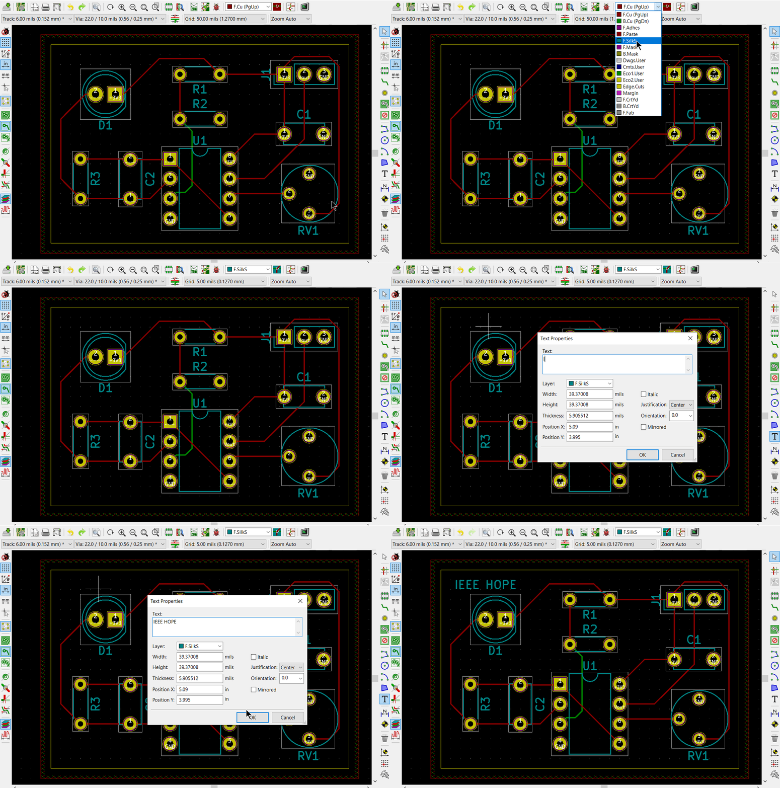
-
Once you are finished, perform a Design Rules Check.
Inspect → Design Rules Checker→ Run DRCor find the ladybug icon in the top toolbar. If you get a pop-up about needing to 'refill zones', click 'OK'.After running DRC, KiCad will warn you if there are any errors with your board. Correct your design and re-run DRC until there are no more DRC violations.
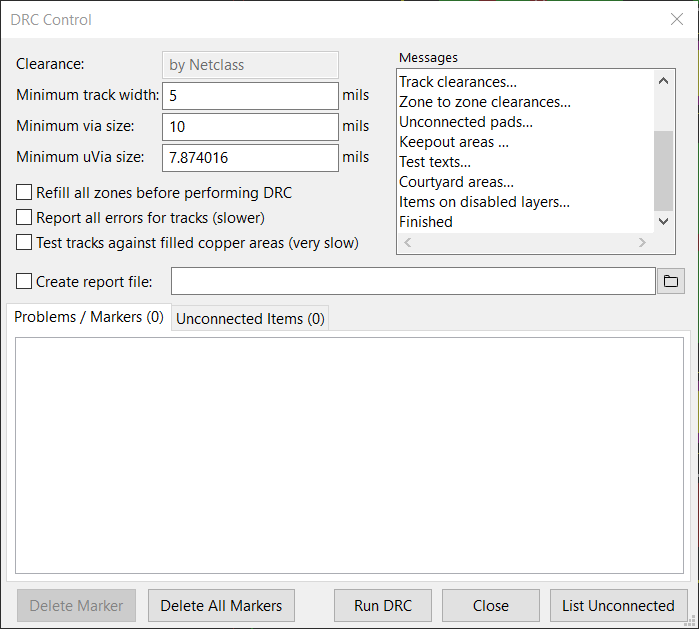
-
Admire your handiwork in 3D!
You can switch the board view with
View → 3D Viewer.
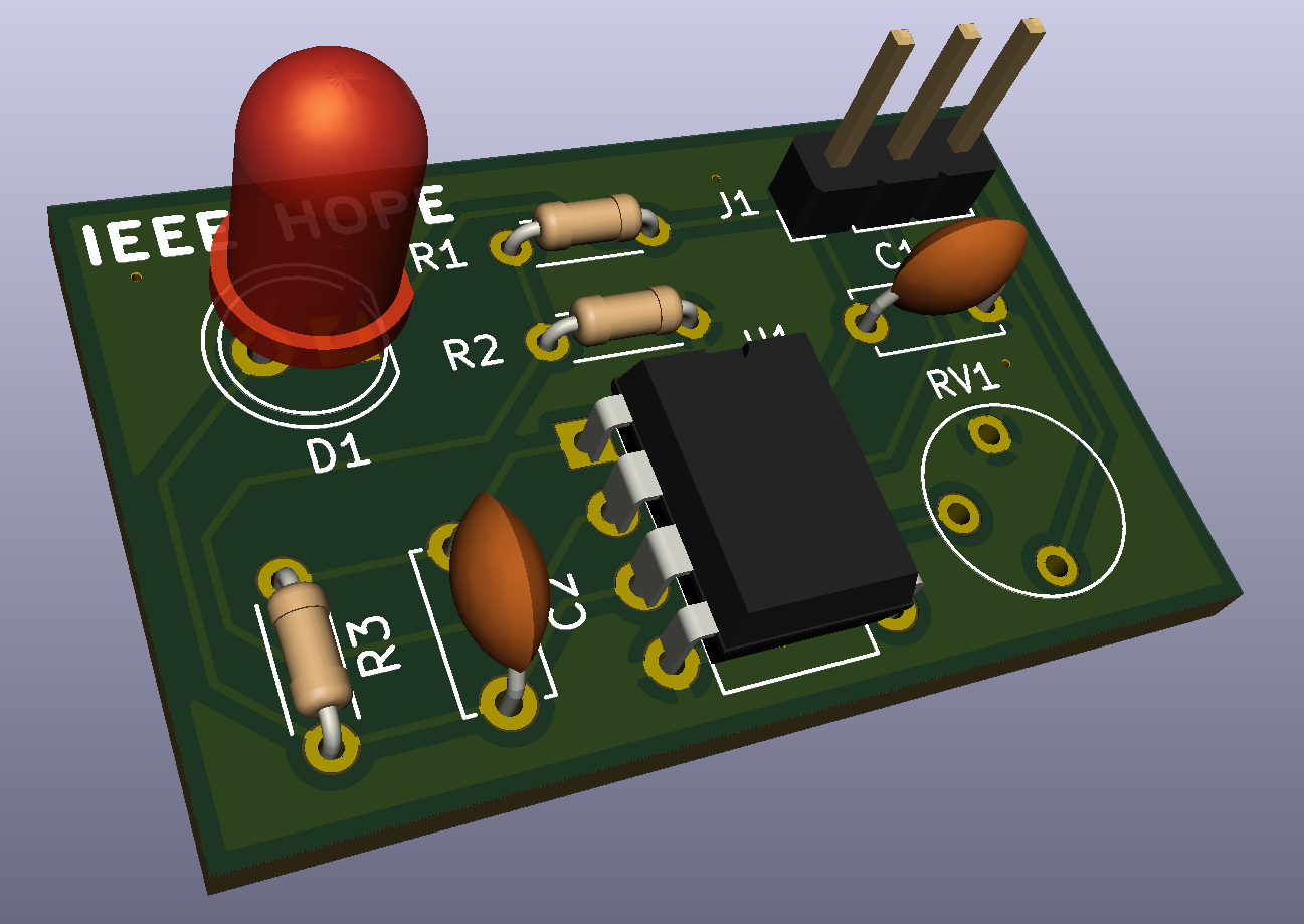
Generating Fabrication Outputs
-
Open up the plot window:
File → Plot. In the upper right-hand corner of the plot window, change the "Output directory" to a new subfolder inside your project folder. Name the new subfolder "outputs" or something of the sort. Click 'yes' if KiCad asks if you want to use relative paths. Then to hit the 'Plot' button at the bottom right corner of the screen. -
(Bottom right corner of Plot window)
Generate Drill Files → Generate Drill File. Don't worry about the options in either output window for now. -
The output files, in their own folder, and now easily packagable to send off to manufacturing! Zip up folder and name it something reasonable.
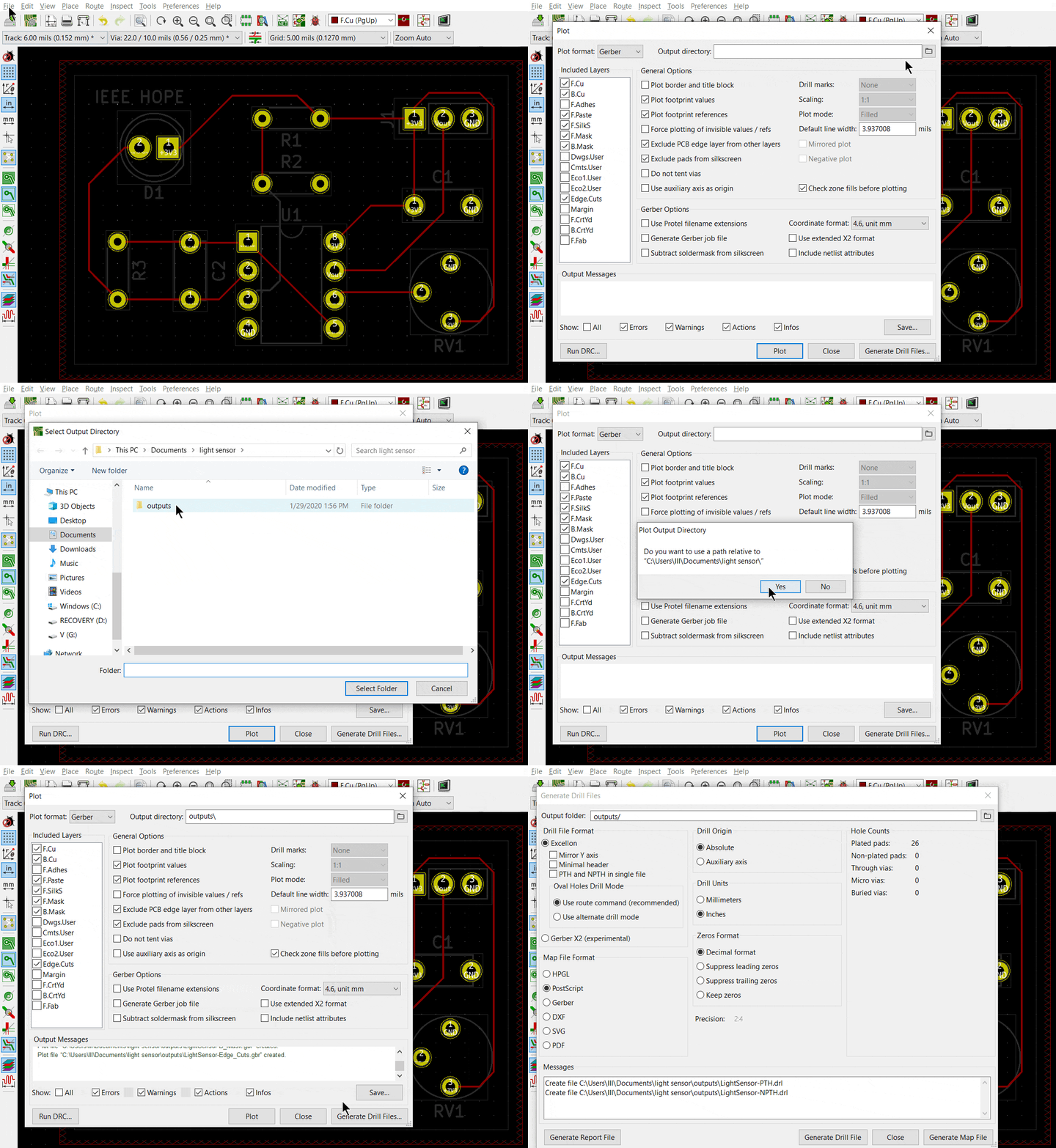
Lab Checkoff
Make sure you have...
-
Completed schematic (match the reference at the top of the page)
-
Completely routed PCB layout (no remaing ratsnest lines, has ground planes, etc.)
-
Some custom silkscreen on the front side of the board
-
Proper board edges defined
-
No DRC errors
-
Generated output files (gerbers: .gbr, and drills: .drl) located in a separate folder from your main project folder
