Why might you want to learn about PCB design?
PCBs are an essential component in electronics. They can be found everywhere, from your phone to your rice cooker, your electric scooters to cars and buses and trains and possibly anything else you can think of. Learning how to make your own PCBs is an essential skill for electrical engineers, researchers, makers and of course, the college student looking forwards to joining the hardware team in one of their school's engineering project clubs.
Course (recommended) prerequisites:
Basic understanding of electricity, electronic circuits, and their diagrams, as well as some experience working with actual electronic hardware.
What is a PCB?
Certainly a pertinent question for those looking to learn about how to make them. The acronym PCB stands for: Printed Circuit Board. why was this name chosen? Very simply: a PCB is a board that implements a circuit and was printed, somehow. More information about the manufacturing of PCBs will be covered later. Now, to properly answer the original question, we will answer the following, related question:
What does a PCB do?
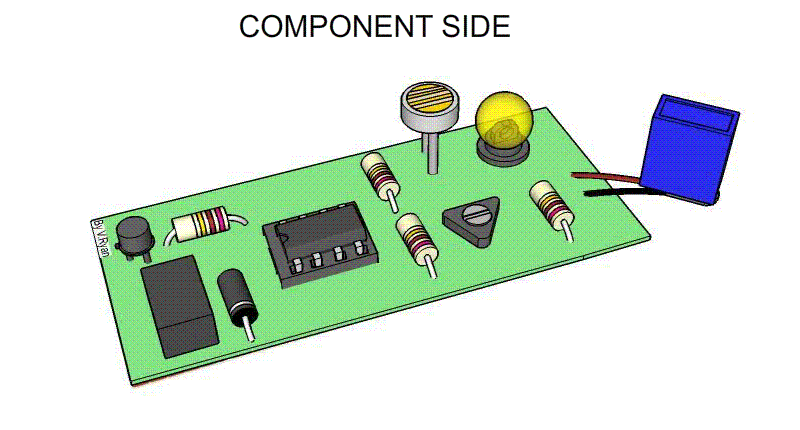
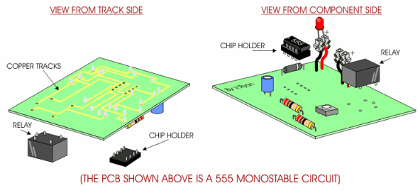
The PCB, as its name implies, is a circuit board. In other words, a PCB is a kind of board that implements the connections and sometimes even components of an electrical circuit, as well as providing a fixed form and structure. The electrical connections between components are made inside of a stiff board; the PCB also provides the connection pads for the components to be both mechanically and electrically attached to the board. In this way it can keep things neat and tidy but also simple.
PCB Alternatives
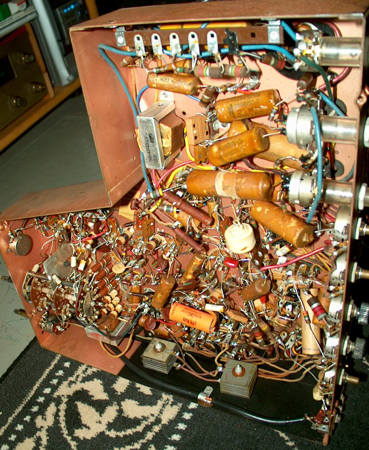
Now, there are certainly ways to implement electronic circuits without PCBs. Back before the advent of the PCB, there was, well, just wires. Behold, point-to-point wiring in an old-timey TV:
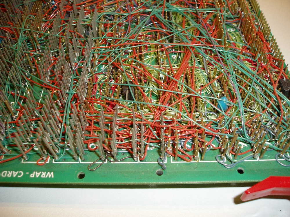
Sometimes, using a solid substrate to provide support for the connections is a good idea (wire wrap board):
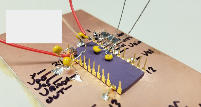
or perhaps you are in a bit of a rush and just need a single IC to work, so you attempt a deadbug:
Little Breadboard History
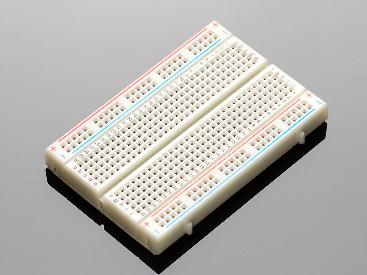
You've probably been introduced to electronics with the infamous white plastic breadboard:
Do you know why they are called "breadboards"? Well, back before these nice little spring-hole breadboards became the defacto standard for electrical prototyping, hobbyists who wanted to build circuits would use a nice solid wooden board to hold their components and help them make the connections. Drill some holes, add metal strips for power terminals, and you'd have a great foundation to work on. And what better option than their mother's breadboard?

Literally, what is a PCB?
TL;DR answer: A PCB is a copper and fiberglass sandwich. The fiberglass part provides stiff structure, while the copper provides the electrical connectivity.
More details will come in the future dedicated to PCB manufacturing details.
PCB Design Tools
Back before computers were commonplace, PCBs often were designed by hand, and every step of the process had to be verified manually. Thankfully, these days there exists many ECAD (Electronic Computer Aided Design) tools for designing PCBs, ranging from completely free (some even completely online!):
- Altium Upverter (online)
- EasyEDA (online)
- Circuit Maker
- KiCAD
- and many more...
to expensive industry professional tools:
- Altium Designer
- Cadence Allegro
- Mentor Graphics Xpedition
- and many more...
There are even integrated Mechanical CAD and PCB ECAD tools, such as
- Autodesk Fusion360
- Dassault Systemes Solidworks
This is by no means an exhaustive list, but just a small sampling of avaliable tools.
In this online HOPE series, we will be using KiCAD, a free, open source PCB ECAD. We suggest using this tool if you would like to follow along with the "hands on" aspect. Of course, you are free to use whatever program you would like, though note that there may be important differences in tool workflow. Occasional glimpses into other tools may be provided in the future lessons.
Basic PCB Design Flow
A very important part of PCB design is when the PCB design tools become relevant in a project. In the typical PCB design process, the basic circuit is already designed. That is,
- the desired function of the circuit can be explicitly expressed
- a rudimentary schematic of the circuit exists
- essential parts of the design have already been researched/decided/tested
before the new project is created in your ECAD.
The PCB, afterall, is in some ways a finalizing component of an electric project. For the PCB itself, it is difficult and possibly even impossible to rework mistakes in either electrical or mechanical aspects. And as for the tools for creating PCBs, they are generally poor options for verifying circuit behavior, especially if digital components are involved. In this way, you should expect a lot of work to happen before you even jump into the schematic editor of the PCB ECAD.
Once in the PCB ECAD, the general process looks like so:
- Create schematic
- Assign footprints (?)
- Import to PCB layout tool
- Group and arrange components
- Route Traces
- Repeat 4-5 a few times
- Create manufacturing outputs
Don't understand what certain steps mean? No worries, just follow along as the HOPE online series goes through the whole process.
next time:
Schematics and Broken Abstraction
the first one with "content" hooray
For the few interested in the history of circuit boards:
https://www.mclpcb.com/history-of-pcbs/
https://www.acdi.com/a-peek-at-the-history-of-pcbs/
Gif source: