By now, hopefully you've gotten used to the basic tools and flow of designing PCBs in KiCad. You're able to generate simple schematics, verify a valid ERC, assign footprints, and move to the layout editor to place and route the components according to a set of Design Rules. But as you move to more difficult boards, you may find that there are some standard tips and tricks, and so far unmentioned or unexplained tools in KiCad, that may help you.
Component Grouping
One of the first things we said about schematics was:
Good schematics show you the circuit. Bad schematics make you decipher them
And then we showed you a bunch of best practices for making your schematic readable and easy to follow. While net labels, minimizing crossing wires, and good use of sheet whitespace / functionality blocking are core ways to keep your schematic clean, they also do something fundamentally important for your layout: tell you how to place your components.
The basic idea is: if we know that a group of components are meant to function together to perform one part of the task (for example: a DC-DC power conversion IC and its supporting passives and diodes), there is no good reason to separate them in the layout. In fact, in most cases, the device designs would like you to place the supporting components as close as possible to the main IC device! (always check the component's datasheet for any guidance on the layout for that part). This means if you properly block out your schematic into the different function areas, you have also mostly figured out how you should group your components together in the layout. During layout, you can think of the grouped components as a form of abstraction. You don't need to always think about the layout as a whole, you can start by only worrying about the layout of each group of components, how they should be oriented in relation to each other, etc.
Let's see how this looks like with an example:
Here we have the microbug layout at the very first stage (only have imported the footprints):
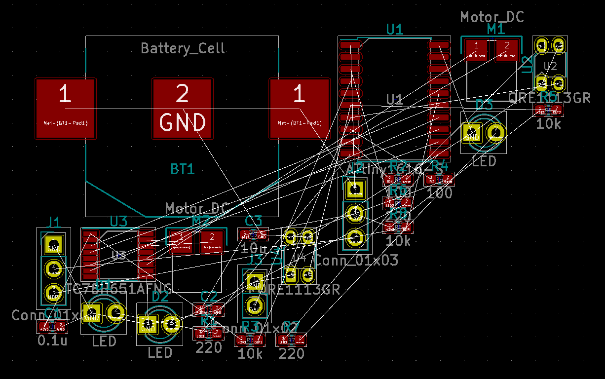
It is quite a mess it seems. You can see how the graphical complexity of boards grow as more parts are added. To start cleaning up this mess, the first thing we will want to do is group the components together. Let's take a look at the reflectance sensors in the schematic:
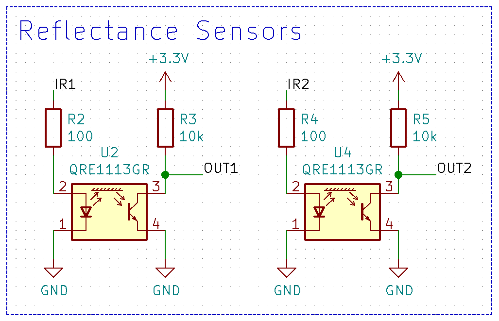
We can see that we'll want to keep R2 and R3 with U2, and R4 and R5 with U4. Now, you can just search around in the layout for the corresponding footprints to R2, R3, etc. But there is an incredibly intuitive way to select these components: cross probing.
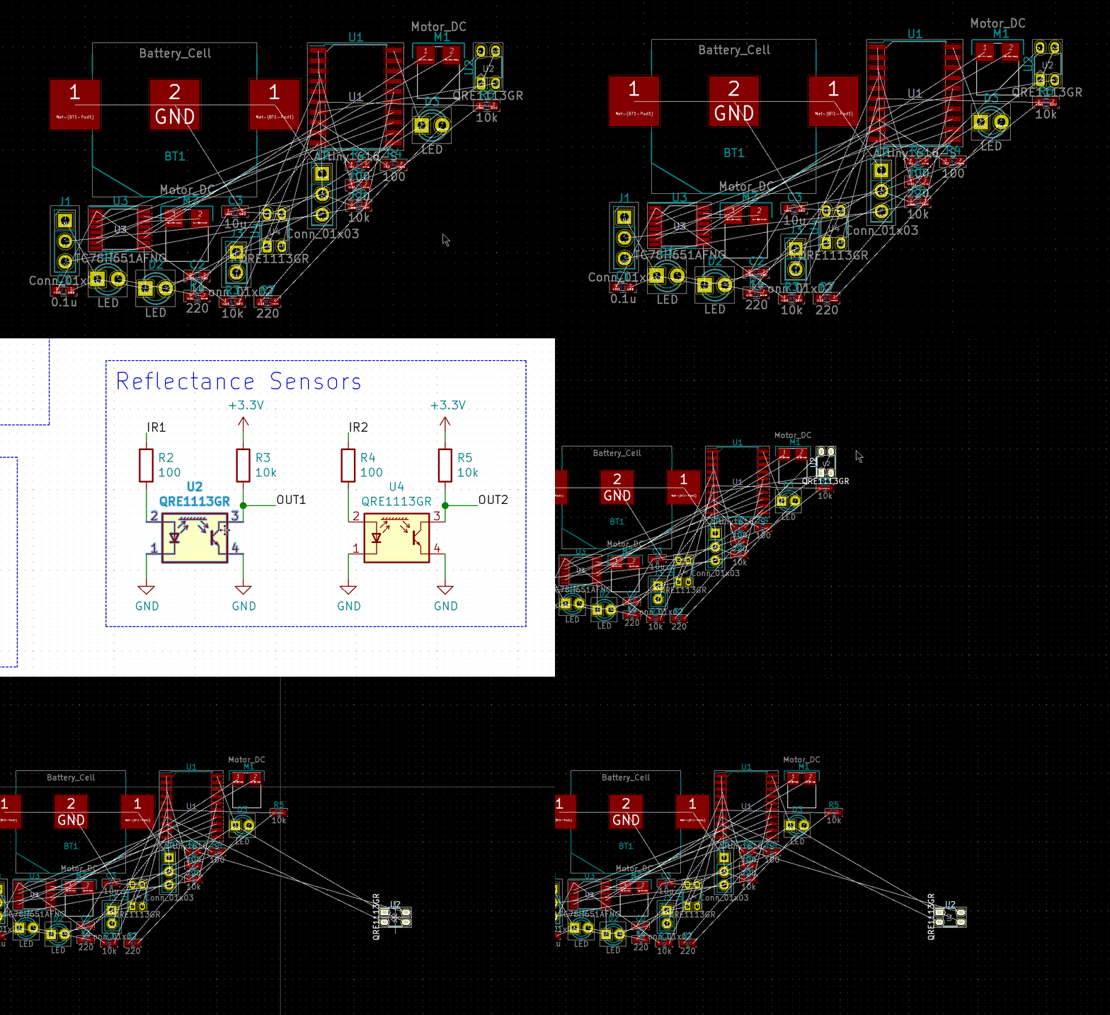
Selecting a component in the schematic editor, will also select it in the layout editor if it is open (This also works the other way around too). This makes it incredibly easy to separate out the parts you want based on your schematic. If you have two screens (or a really large, wide one) to work with, you should set up the schematic editor on side and the layout editor on the other when doing your layout placement.
Once you've got your general placement down in your groups, you can start doing some of the easy routing inside the groups (don't forget to set your grid size smaller when you start routing!). You can think about groups as abstracted components, once the relative routing inside the group is done, you will probably not need to worry about it anymore, and only need to focus on group-to-group routes, which are typically longer tracks.
Making Life Easier
A new feature in KiCad 5.99 also makes keeping groups together as groups, easy. You can now group selected components and tracks together just like you would in applications like Microsoft Powerpoint or Google Slides. When you select a component in a group, the entire group will be selected.
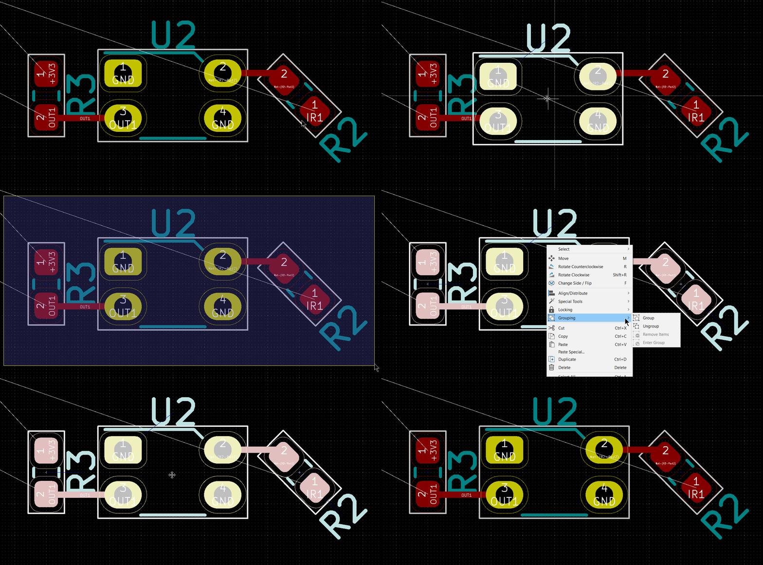
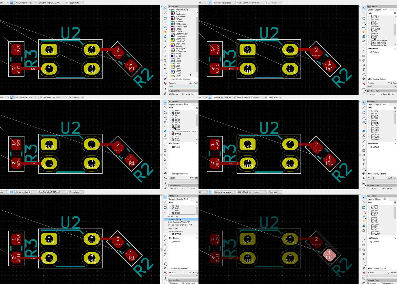
You may have noticed that there were no GND ratsnest lines in the example .gif above. Typically, since GND (and other power rails) are connected not by manual routing but by pours, it will keep things neater if we could hide the ratsnest for these nets. Thankfully, KiCad 5.99 also introduced the ability to toggle on the visibility of nets (in addition to visible of layers, and object types). You can change the visiblity (and do some other neat things, such as highlight the net) in the "Appearance" pane on the right side of the layout editor.
Component Placement
Now that you have nicely grouped components and such, there is still is issue of where to place those. The follow is a short list of things to consider when setting up placement on the board:
- Figure out the placement of external interacting components. This includes things such as connectors/ports, buttons, potentiometers, LEDs, etc. Especially if the mechanical design of the project is already decided or is happening in tandem with the PCB, getting the correct placement of these kinds of parts first is essential and will save you time later.
- Cluster component groups based on power (parts using 12V should stay together, parts using 5V should stay together, etc.)
- Orient and position your components in such a way to minimize the length of the the required traces and the number of vias. This goes for both within a group, and between groups. You should only use vias when necessary, so try to place and orient to support that goal.
- Many ICs' datasheets will have suggested layouts or noted recommendations. Make use of your component's datasheets!
- Keep aware of the physical size of components, and their closeness to each other. Think about how to make your life easier when assembling the board or in the case of rework.
Selection Filters and Visibility
Selection Filters
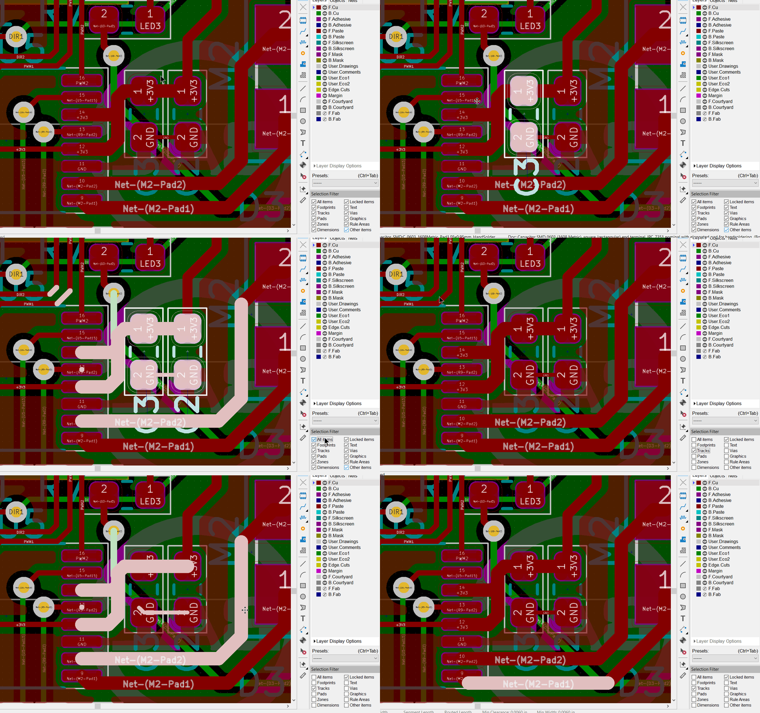
Sometimes, you are in the middle of your layout work and you have a lot of things at the same location. It makes it hard to select exactly what you want. KiCad 5.99 has a solution for the problem in the bottom-right pane: Selection Filters. These allow you to choose what you want to be selectable, such as only tracks, or everything but text objects, etc.
Locking Layout Objects
Sometimes, an object type selection filter isn't what you need. Sometimes you have some part perfectly laid out, or perfectly set to some dimension, and you don't want to be able to accidentially change it when you are working on other parts of the layout close to that area. You can lock layout objects (or entire groups) to prevent unintended edits:
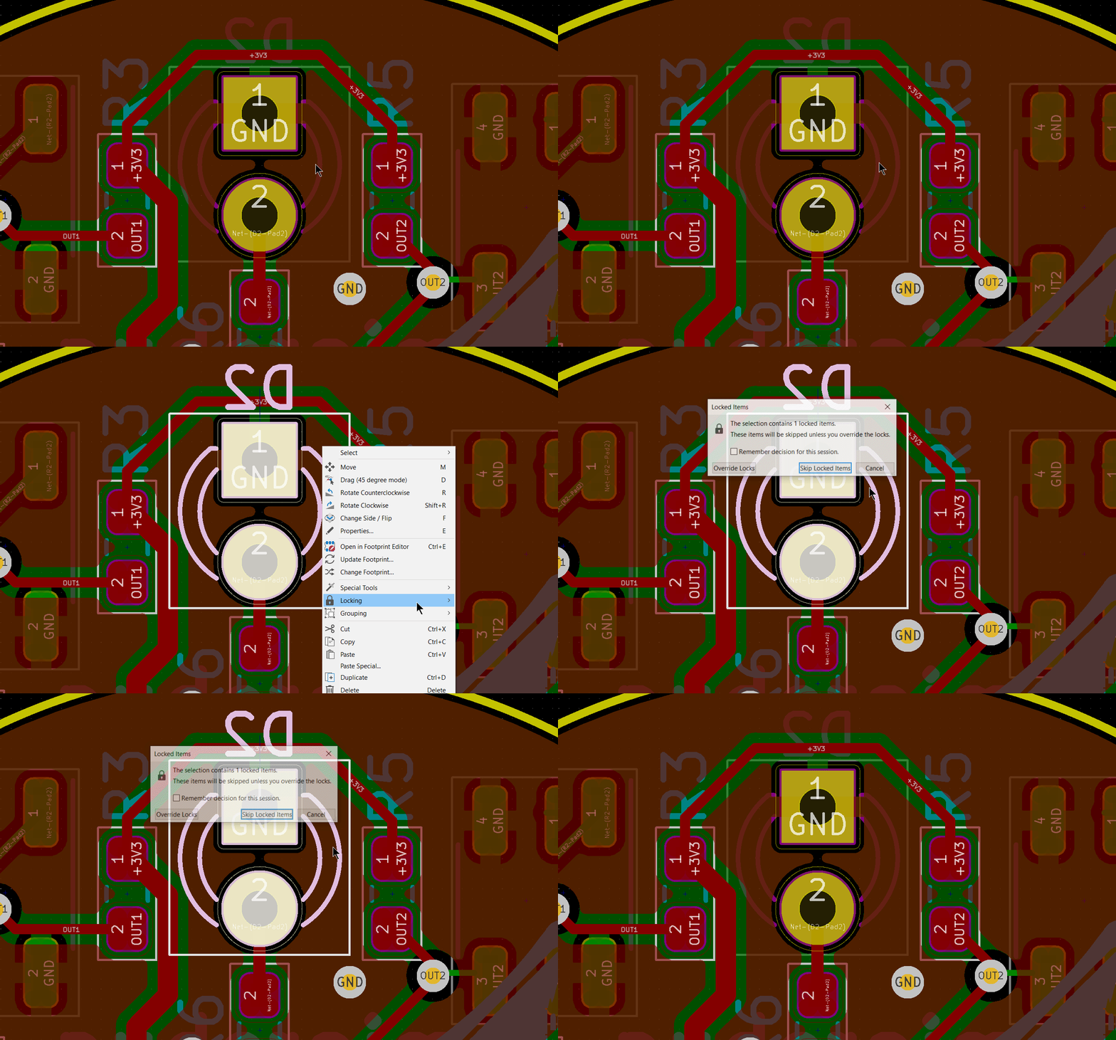
You can quickly toggle a selection between locked and unlocked with the shortcut key 'L'.
Contrast Mode and Hiding Layers
Even with filtering and locking, it might be difficult to see what you are working with. Maybe too many text objects are in the way, or things from the other layers are cluttering your viewport and making it hard to discern the optimal routing path on your current layer. In these cases, it may help to hide unnecessary layers, or isolate your view specifically to the layer you are working on.
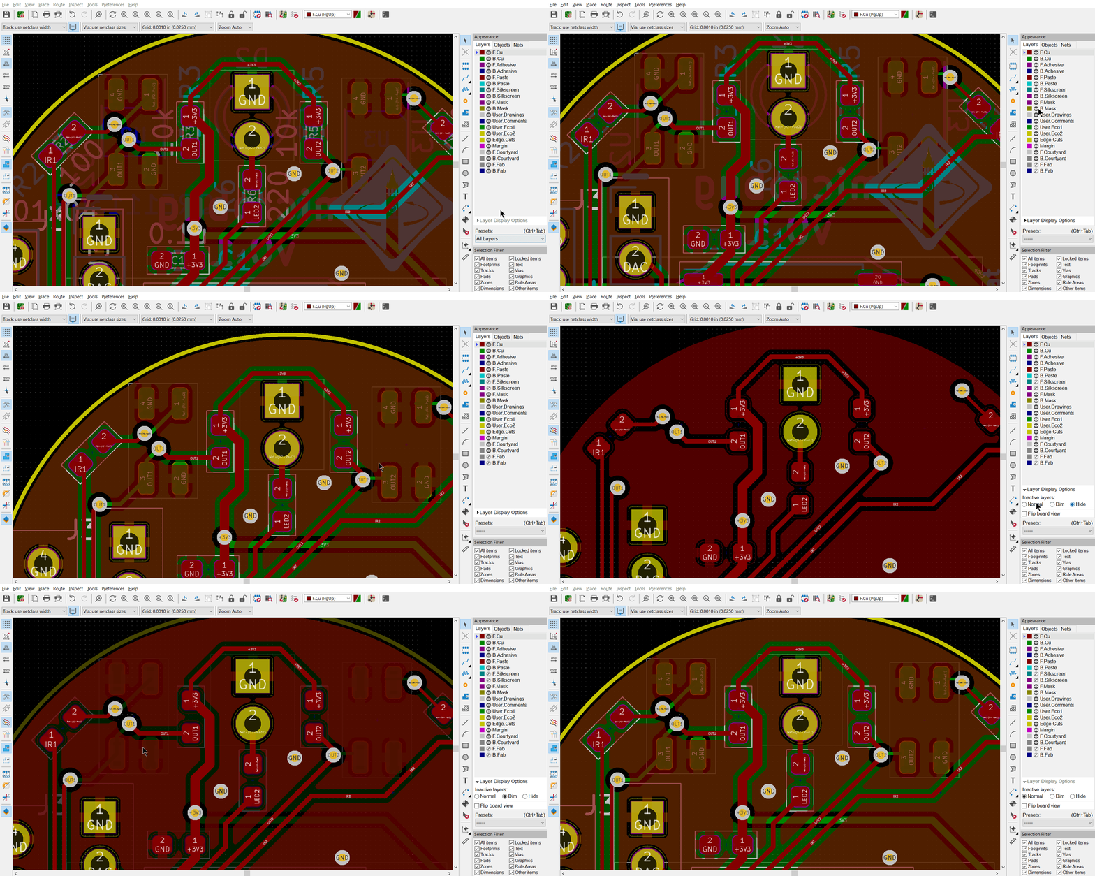
You may find the layer visibility presets under the "Presets" dropdown useful for swapping between different board layer views.
Track Widths and Net Classes
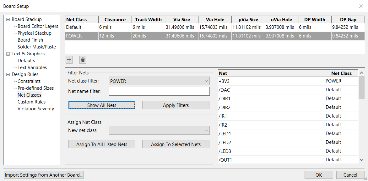
The standard 10mil track is pretty great for making general connections, but sometimes you need something different, whether it be for impedance matching purposes, space constraints, or power and heat concerns. In these cases, you could manually change the track width using the dropdown in the top left, but it would be easier if KiCad could automatically switch for you. For this, you can use Net Classes. Net classes are a way to organize your nets into different classes, allowing you specify different standard routing widths (and a few other things) for different classes of nets. For example, you can have a collection of Power Nets, with a standard routing width of 40mil and clearance rule of 12mil instead of the default 10mil and 6mil, for your high power nets 12V and 5V in a power circuit.
Routing w/ Zones and Keepouts
Sometimes though (especially with power circuits), you want to maximize the amount of copper a net connection has. You could draw individual shapes or tracks, but the easiest and best solution would be to use polygon pours (yes, the exact same thing for your ground planes). Many power IC circuits will typically have their suggested layouts shown with pours (example from the MP2307 datasheet):
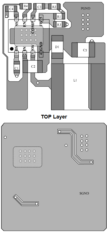
So for anything high current (and potentially high heat), using pours instead of simple track objects will be the way to go. Typically coupled with these pours are arrays of vias to a similar pour on the other side of the board to increase surface area and physical dimensions of the conductor (you can see this in the layout above in the ground plane).
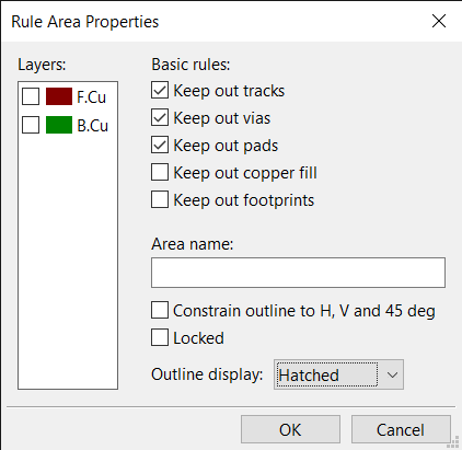
The other kind of zone you can use is the keepout zone (rule area). These zones do exactly as their name implies: keep out features. Sometimes certain components need extra space from other copper for electrical reasons, mechanical pieces may take up parts of the board, etc. and these keeps can help you enforce these constraints. They are drawn exactly the same way as copper pours.
Other Neat Features
Cleanup Tools
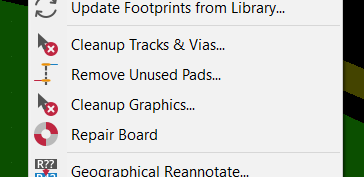
KiCad 5.99 has also introduced a few automated tools to "clean up" your layout. Of the most use may be the "Cleanup Tracks and Vias" tool, which helps remove a few common layout issues such as track segments stuck under pads, accidental cross net shorts, and antenna traces/vias (a trace or via that doesn't connect to anything else). Giving it a quick run will usually help clear up some DRC warnings or errors related to such routing garbage.
Dimensioning
In the case that you need specific dimensions visible in your layout (for example, certain component(s) must be in a very specific location), you can add dimensions to User.Drawings (or Eco layers) using the dimension tool.
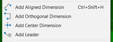
There are a few different types of dimensions avaliable to use, and if you're familiar with mechanical CAD software it should be quite clear what each kind does. However, the dimensioning tool is not used for precise placement of components or other board features. Such placement should be done by adjusting the grid, changing the grid origin, and using the relative distances (dx, dy) at the bottom of the window. To use the relative distances, pressing space will set the temporary origin.
For complicated physical board designs, the board restrictions should be determined outside of KiCaD in a mechanical CAD software, and imported via DXF file into KiCaD.
Plugins
KiCad allows the use of external plugins to augment the functionality of the software (for both the schematic editor and layout editor). These plugins are written in Python imported by adding them to KiCad's external plugins folder. Although we will not be using any plugins during HOPE, feel free to explore what exists on the web (just note that most plugins have not been designed to work with version 5.99) or even look up the scripting documentation.
