


Footprint Creation
Footprints are stored in libraries just like KiCad symbols. For the component footprints you create, we recommend adding the parts to a project library.
Note: Do NOT add standard passives to your library (i.e. external capacitors, resistors for ICs). DO add the passive if it has a special shape (i.e., a high wattage resistor).
Something to think about: Why might, in a collaborative environment, using project libraries instead of global libraries be a good idea?
- Open up your footprint editor from the KiCad home window:

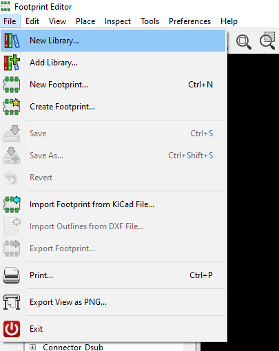
- Create a new footprint Library by doing File → New Library. Make sure to select "Project" in the "Select Library Table" window.
Note how the footprint library is saved. A folder with a custom extension!
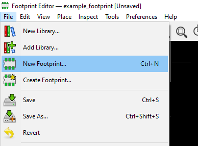
- Create a new footprint for a part you have chosen and add it to the footprint library you had just created (KiCad will prompt you if you try saving).
KiCad has a bunch of simple footprint generators ("File->Create Footprint...") for standard-like footprints (and decorative layout elements), which we suggest you try out, just to know it exists. Make sure to double check the footprint it creates though!
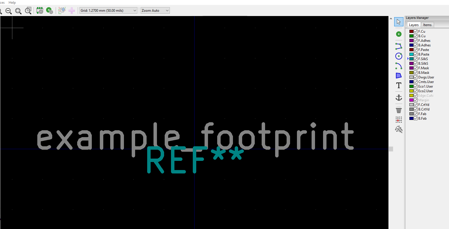
This should start you off very similarly to symbol creation, with only a reference designator (on the Front Silkscreen layer) and the footprint name (on the Front Fab layer) in an otherwise empty grid.
- The process for creating footprints is as so:
- Place and dimension component pads
- Draw important silkscreen
- Draw component courtyard region
- Anything else: assembly data, 3D model
You should have the component's datasheet open to the page on its physical dimensions for whatever component package you have chosen to use before starting.
We highly suggest watching Digikey's Footprint Creation Tutorial. Start from 5:51. If you have some time, the entire series is a good walkthrough of the KiCad/PCB design process. Note however, that the video tutorial was made using an older version of KiCad, and thus certain features have been changed since then.)
We do not recommend remaking standard packages that already exist in the default footprint libraries KiCad provides.
Quick Footprint walkthrough
Some important tidbits before you begin:
- Make correct use of the origin to make rotation and placement more intuitive.
- Choose a grid size that makes sense for the footprint you are making. Because this is representative of a real part, maintaining a regular grid size is unnecessary.
- At the very least, make the relative dimensions between the pads, as well as the pad sizes, accurate to the datasheet recommendation.
You may want to move the default designator and name text out of the origin before you begin.
There are some visualization tools in the left toolbar. Toggle them on and off to see what they do, and how they might be helpful.
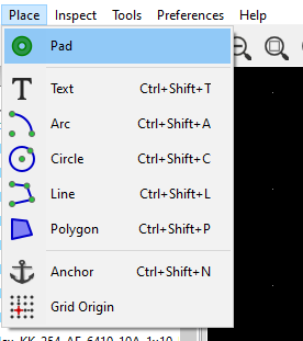
Placing Pads
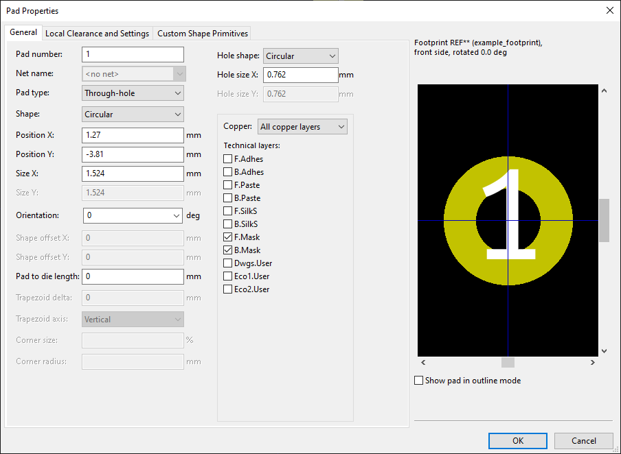
- Just like symbol creation, we start with the pads (pins in the symbol). Notice that pad placement happens on the defined grid. One tip to make the pad placement process easier is to set the grid to the desired spacing.
- Opening up the pad properties opens a similar window to the pin properties found in the symbol editor, but with pad-specific features, such as pad type, shape, size, and layers. Here, you can set the position of the pad precisely. In most cases you will not need to worry about changing the layers, as the Pad type will select the right ones for you.
-
Place the rest of the pads in the correct spots. The Measure tool may be helpful to verify placement. Note that you can hold down the Alt key to disable grid-snap, or Ctrl to snap to 45 degree angles.
-
The next few steps will involve using the graphic tools. These work exactly the same in all board layers; the board layer determines what the actual result is.
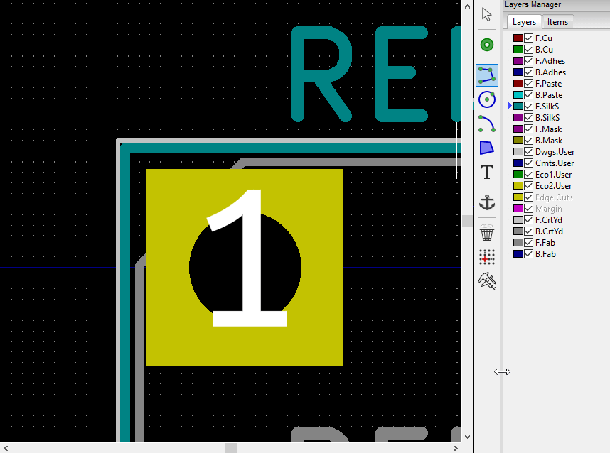
- Put elements in the Front (or back) silkscreen layer (F.SilkS) to help visualize your part. The most important element of the silkscreen is the orientation mark, which is usually a dot next to the pin 1. You may find other forms for different kinds of components.
- Draw the general body of the component in the Fabrication layers. This is a meta data layer mainly for automated assembly use, but you can use it for generating the general shape to use as a base for the graphics on other layers, such as adding a silkscreen outline or component courtyard.
- Add a component courtyard. This is the 2D area that KiCad uses to determine whether two components will physically collide.
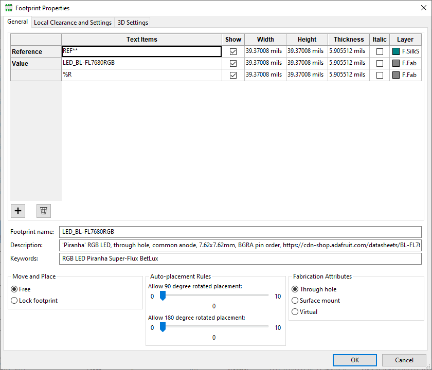
- You can change the footprint properties (name, description, keywords) and add more info, such as a 3D representation of the component, using the Footprint Properties window (Edit -> Footprint Properties).
Using pre-existing footprints
In addition to creating footprints yourself from component datasheets, you may also find component footprints (as well as symbols, or even entire part libraries such as the Digikey KiCad component library) online. There are a multitude of tools at your disposal: feel free to use any of them but make sure to always double check any footprint found online.
How to import KiCad footprints
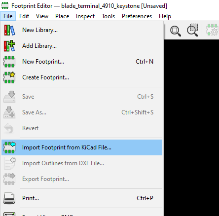
- Download the footprints (must be for KiCad v4+) and uncompress them if needed.
- File → Import Footprint from KiCad File. Select the .kicad_mod footprint file that you would like to use.
- Double check the imported footprint.
- Save the footprint to your project footprint library.
How to import KiCad footprint libraries
This is useful for when you need an entire library of component footprints, such as Digikey's footprint library.
- File → Add Library (its like, the "New Library" symbol but with a plus + sign)
- Select the footprint library folder.
- Add the library either to the Project or Global library table.
- Money